Обработка полупроводников с ЧПУ | Услуги прецизионной обработки
Yijin Solution makes super precise parts for semiconductor manufacturing. Our machines accurately cut materials to get the most out of them. We work in really clean spaces to keep things like dust totally away from your parts.
- ⬤Сервис
- ⬤Ваши данные
- ⬤Отправить


Что такое обработка с ЧПУ полупроводникового оборудования?
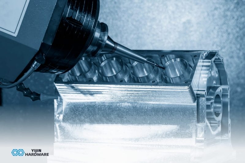
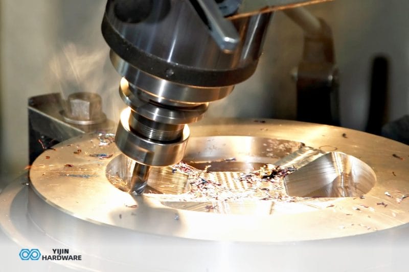
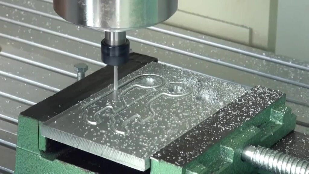
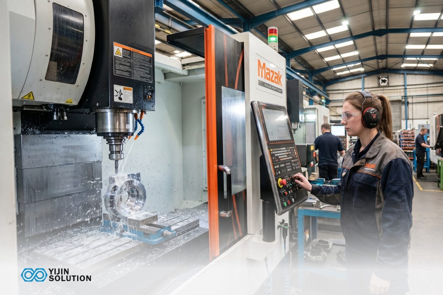
Полупроводник Обработка на станках с ЧПУ связано с изготовлением сверхточных деталей для компьютерных чипов. Это также относится к электронике. Мы используем станки, управляемые компьютерами, для резки материалов на необходимые детали.
Затем эти детали попадают в машины, которые производят чипы. Мельчайшие проблемы могут испортить дорогостоящие полупроводниковые устройства, поэтому мы работаем в очень чистых помещениях.
Основные преимущества
- Сверхточная резка
- Чистые производственные условия
- Работает со специальными полупроводниковыми материалами
- Компьютерное управление для идеальной повторяемости
Рынок полупроводникового оборудования достигнет $223,8 миллиарда к 2029 году. Наши передовые возможности станков с ЧПУ помогают производить детали, которые обеспечивают работу этой быстро развивающейся отрасли.


Какие полупроводниковые компоненты мы можем обрабатывать?
Yijin Solution manufactures precision semiconductor components with superior surface finishes that exceed SEMI standards. Our CNC machining solutions include:
Компоненты для обработки пластин:
- Патроны и держатели для вафель: Сверхплоские поверхности (плоскостность <0,001 мм) для надежного удержания пластин во время обработки
- Душевые насадки для CVD: Прецизионно просверленные микроотверстия из нержавеющей стали или латуни для равномерного распределения газа
- Формы для полировальных кругов: Замысловатые алюминиевые формы для полиуретановых полировальных подушечек, используемых при производстве полупроводников
Компоненты для тестирования и измерений:
- Испытательные гнезда: Сложные геометрии для проверки работоспособности полупроводников с отверстиями для вставки pogo pin
- Карты-зонды: Высокоточные центровочные приспособления для тестирования полупроводников
- Приспособления для декапсуляции: Механические приспособления для обнажения внутренних компонентов
Тепловое управление:
- Радиаторы: Сложная геометрия ребер с максимальной площадью поверхности (на 40% эффективнее стандартных конструкций)
- Компоненты теплового интерфейса: Прецизионные поверхности для оптимального теплового контакта
- Каналы жидкостного охлаждения: Внутренние микрофлюидические структуры для усовершенствованного охлаждения
Поддержка и структура:
- Конечные исполнители: Легкие алюминиевые кронштейны для перемещения пластин
- Корпуса для полупроводников: Экранирование электромагнитных помех и защита от загрязнений
- Оборудование Рамы: Высокоточные монтажные системы для оптической юстировки


Какие материалы могут использоваться для изготовления полупроводниковых компонентов?
Полупроводниковые компоненты требуют специализированного материалы with specific electrical, thermal, and mechanical properties that we expertly mill at Yijin Solution.
| Материал | Свойства | Приложения | Проблемы обработки |
|---|---|---|---|
| Кремний | Полупроводниковый, хрупкий | Пластины, МЭМС | Микротрещины, термочувствительность |
| Карбид кремния | Теплопроводность: 370 Вт/мК Твердость: 9,5 Мооса | Силовая электроника | Сильный износ инструмента, медленная обработка |
| Арсенид галлия | Подвижность электронов: 8500 см²/Вс | Радиочастотные компоненты, оптоэлектроника | Токсичность, хрупкость |
| Германий | Зазор: 0,67 эВ | Инфракрасная оптика, транзисторы | Низкая температура плавления, хрупкость |
| Глиноземистая керамика | Диэлектрическая прочность: 16,9 кВ/мм | Подложки, изоляторы | Износ инструмента, определение кромки |
Передовые металлы:
- Нержавеющая сталь 316L: Вакуумная переплавка для сверхвысокой чистоты
- Хастеллой (C22, C276): Превосходная коррозионная стойкость для систем подачи газа
- Титановые сплавы: Отличное соотношение прочности и веса для структурных компонентов
- Твердосплавная оснастка: Используется для режущих инструментов в самом процессе обработки
Специализированные полимеры:
- PEEK: Температурная стойкость до 250 °C и отличная химическая стабильность
- Полиимид: Превосходные электроизоляционные свойства
- Ultem (PEI): Высокая термостойкость и стабильность размеров
- PPS: Отличная химическая стойкость для компонентов влажной обработки
Как мы обеспечиваем качество полупроводников?
Yijin Solution maintains semiconductor-grade quality control through ISO-certified inspection procedures and SEMI-compliant processes.
Производство в чистых помещениях:
- Среды ISO 4-7 (класс 10-10 000)
- HEPA-фильтрация с эффективностью 99,99%
- Непрерывный мониторинг частиц до 0,1 мкм
- Безопасные для электростатических разрядов материалы и оборудование
- Протоколы для персонала, включая соответствующую одежду
Передовые измерительные технологии:
- Координатно-измерительные машины (КИМ): Точность до 0,1 мкм
- Оптическая и лазерная профилометрия: Анализ поверхности до Ra 0,05 мкм
- Видеоизмерительные системы: Бесконтактная проверка размеров
- Электронная микроскопия: Анализ поверхности на микронном уровне
Рабочий процесс качества:
- Предварительное производство:
- Сертификация и прослеживаемость материалов
- Проверка и утверждение первого изделия
- Проверка параметров процесса
- Внутрипроизводственный контроль:
- Контроль статистического управления процессами
- Проверка размеров в режиме реального времени
- Мониторинг параметров окружающей среды
- Окончательная проверка:
- Проверки на соответствие стандартам SEMI S2/S8/S30
- Полная отчетность по измерениям
- Проверка чистоты поверхности для обеспечения гладкости поверхности


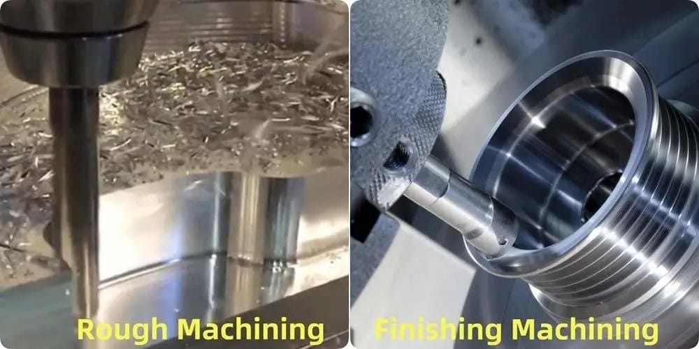
Чем отличается обработка с ЧПУ для полупроводников?
Прецизионная обработка полупроводников с ЧПУ требует значительно более высоких стандартов точности и чистоты, чем обычная обработка и сборка.
| Требование | Стандартная обработка | Обработка полупроводников |
|---|---|---|
| Типовые допуски | ±0,005″ до ±0,030″ | ±0,0005″ до ±0,005″ |
| Отделка поверхности | Ra 1,6-3,2 мкм | Ra 0,05-0,8 мкм |
| Чистота | Промышленность | Чистое помещение ISO 4-7 |
| Чистота материала | Коммерческий класс | Полупроводниковый класс |
Критические различия:
Требования к точности
- Точность позиционирования в пределах 0,001 мм (1 мкм)
- Биение шпинделя менее 0,002 мм
- Термическая стабильность в пределах 0,5 °C
- Контроль вибрации с амплитудой менее 0,1 мкм
Материальные проблемы
- Хрупкие полупроводниковые материалы требуют специальных приспособлений
- Режущие инструменты требуют постоянного контроля для достижения стабильных результатов
- Предотвращение микротрещин при токарной и фрезерной обработке с ЧПУ
- Беспроблемные методы монтажа крупных деталей
Управление процессом
- Контроль параметров в режиме реального времени
- Оптимизация траектории движения инструмента для снижения напряжений
- Управляемые профили ускорения/замедления
- Усовершенствованное программирование CAD/CAM для сложных геометрических форм
Каковы допуски и обработка поверхностей для полупроводниковых компонентов?
Полупроводниковые устройства требуют чрезвычайно жестких допусков и превосходного отделка поверхности для правильного функционирования в критически важных производственных процессах.
| Тип компонента | Типичный допуск | Отделка поверхности | Плоскость |
|---|---|---|---|
| Вафельные патроны | ±0,0005″ (0,0127 мм) | Ra 0,05-0,2 мкм | 0,001 мм |
| Испытательные гнезда | ±0,001″ (0,0254 мм) | Ra 0,2-0,8 мкм | 0,005 мм |
| Теплоотводы | ±0,002″ (0,0508 мм) | Ra 0,8-1,6 мкм | 0,01 мм |
| Корпуса | ±0,005″ (0,127 мм) | Ra 1,6-3,2 мкм | 0,05 мм |
Технические характеристики отделки поверхности:
- Зеркальная отделка: Ra 0,05-0,1 мкм для компонентов фотолитографии
- Тонкая отделка: Ra 0,2-0,8 мкм для уплотнительных поверхностей
- Стандартная отделка: Ra 0,8-1,6 мкм для общего применения
- Функциональная отделка: Ra 1,6-3,2 мкм для некритичных поверхностей
Расширенные возможности допуска:
- Параллельность: 0,002 мм на поверхности 300-миллиметровых пластин
- Перпендикулярность: 0,005 мм для критических монтажных интерфейсов
- Концентрация: 0,003 мм для выравнивающих элементов
- Допуск профиля: 0,008 мм для сложных 3D-поверхностей
Измерение и проверка:
- Стандарты ASME Y14.5 GD&T
- Геометрический допуск ISO 1101
- Спецификации SEMI P1-92 для обработки поверхности


Влияние закона CHIPS на производство полупроводников
Закон о CHIPS и науке от 2022 года изменил полупроводниковую промышленность США, создав беспрецедентные возможности для механической обработки в полупроводниковой промышленности. Этот закон позволил привлечь сотни миллиардов государственных и частных инвестиций для укрепления отечественного производства.
Ключевые события в отрасли:
- $52,7 миллиарда федеральных средств на исследования и производство полупроводников
- 30% инвестиционный налоговый кредит для производителей оборудования
- Создание региональных производственных центров
- Сосредоточьтесь на создании комплексных экосистем цепочек поставок
How Yijin Solution Supports CHIPS Act Goals:
- Производство в США (760 NW 10th Ave, Homestead, FL 33030) обеспечивает внутреннее производство.
- Специализация в области обработки с ЧПУ для полупроводниковой промышленности
- Поддержка как известных производителей полупроводников, так и новых инноваторов
- Передовые возможности, соответствующие технологиям следующего поколения 3 нм и выше
Проблемы отрасли, которые мы решаем:
- Растущие требования к миниатюризации расширяют границы точности
- Сложности обработки материалов при производстве полупроводников
- Предотвращение риска загрязнения во время травления и других процессов
- Экономичные производственные процессы для повышения точности и эффективности
Являясь квалифицированным поставщиком, располагающим производственными мощностями как в США, так и в Китае, мы помогаем ведущим компаниям полупроводниковой промышленности удовлетворять как производственные потребности, так и требования закона CHIPS о внутреннем содержании.
Why Choose Yijin Solution for Semiconductor CNC Machining?
Yijin Solution delivers unmatched high-speed semiconductor CNC machining capabilities with ISO-certified precision and comprehensive SEMI standard compliance. Our multi-axis CNC systems achieve the level of precision required in semiconductor production for critical components, while our ISO-classified cleanroom facilities ensure contamination-free manufacturing essential for semiconductor performance.
Наши конкурентные преимущества:
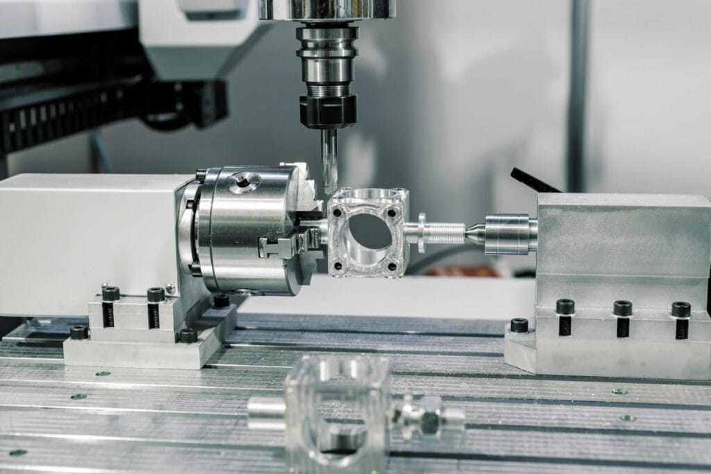
- Расширенные возможности 5-осевой обработки для сложных геометрических форм полупроводников
- Экспертиза материалов охватывает кремний, SiC, GaAs, керамику и специализированные металлы
- Чистые производственные помещения ISO 4-7
- Полное соответствие стандартам SEMI S2/S8/S30
- Возможности контроля на микронном уровне с помощью передовой метрологии
- Жесткие строительные машины портального типа, способные выдерживать очень жесткие допуски
With facilities in both China and the United States (760 NW 10th Ave, Homestead, FL 33030), we provide responsive local support with global manufacturing capabilities. Our systems are optimized to machine parts faster while maintaining the stringent quality standards required for success in the semiconductor manufacturing industry. Partner with Yijin Solution for solutions for the semiconductor industry manufactured with the precision, quality, and cleanliness your advanced applications require.

Что говорят наши клиенты


Часто задаваемые вопросы по обработке полупроводников с ЧПУ
Yijin Solution achieves tolerances ranging from ±0.0005″ (0.0127 mm) to ±0.005″ (0.127 mm) for semiconductor parts. The specific tolerance capabilities depend on the material being machined, component geometry, and feature size. Critical alignment features on wafer chucks and optical components often require the tightest tolerances (±0.0005″), while structural elements may allow for standard tolerances (±0.005″). Our advanced CNC technology maintains dimensional stability throughout the machining process, ensuring consistent precision for your semiconductor component requirements.
Мы предотвращаем загрязнение с помощью комплексных протоколов чистых помещений и специальных процедур обработки материалов на протяжении всего производственного процесса. Все полупроводниковые компоненты производятся в чистых помещениях ISO 4-7 (класс 10-10 000) с фильтрацией HEPA, положительным давлением и строгими протоколами для персонала, включая соответствующую одежду для чистых помещений. Материалы проходят очистку и проверку перед поступлением в производственную среду, а специализированные упаковочные системы поддерживают чистоту во время транспортировки. Наши меры по контролю загрязнения включают регулярный подсчет частиц, анализ остатков на поверхности и сертификацию чистых помещений, чтобы гарантировать, что ваши компоненты останутся нетронутыми.
Обработка с ЧПУ обеспечивает превосходный контроль и точность по сравнению с кислотным травлением или лазерными методами для полупроводниковых компонентов. В отличие от химических процессов, которые сложно точно контролировать, наши решения с ЧПУ обеспечивают стабильные, повторяющиеся результаты с точным контролем глубины. Даже малейшее отклонение в производстве полупроводников может привести к катастрофическим сбоям, но наши процессы обработки обеспечивают геометрическую точность до ±0,0005″. Наше оборудование специально разработано для обработки сложных полупроводниковых геометрий с сохранением целостности материала - то, что лазерные процессы могут нарушить из-за зон термического воздействия. Являясь краеугольным камнем производства полупроводниковых компонентов, наша приверженность к совершенству в механической обработке обеспечивает превосходное качество обработки поверхности, более жесткий контроль размеров и лучшее определение кромок по сравнению с химическими или термическими альтернативами.
Ресурсы ЧПУ
How to Use Yijin Solution Online Quoting Platform
Getting a custom part quoted should not feel complicated. If you already have a drawing or 3D file ready, Yijin
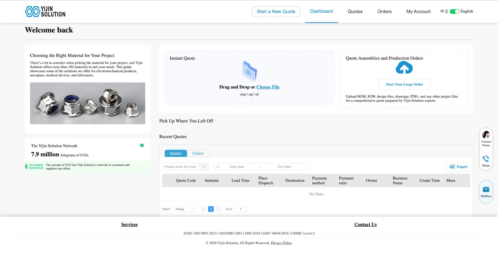
Yijin Solution Launches an Online Quoting Platform
Yijin Solution has launched its new Online Quoting System, giving customers a simpler way to upload files, review pricing, and
What is a CNC Machining Certification? Types, Requirements & Industry Standards
A CNC machining certification is a documented standard that defines how a machining supplier operates. It covers process control, material
Начните сегодня. Быстрое изготовление деталей.
Бесплатное проектирование механически обработанных деталей для ваших проектов с быстрыми сроками выполнения.
